
v1.5 Home | v1.5 Kit | v1.5 Schematic Guide (20 Dec. 2002) | v1.5 Construction Guide | v1.5 Software
Here are notes to help you understand how the TE-WB works. It also servers as a reference if you are constructing the version 1.5 PCB. Please note that all images and text are Copyright 2002 © Tech Edge Pty Ltd.
|
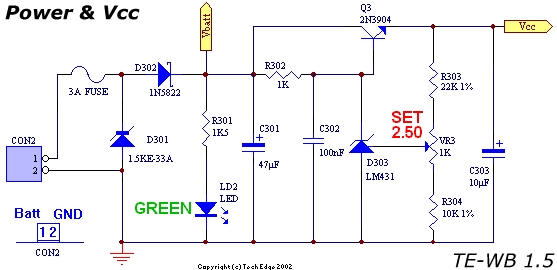
The power connector CON2 has pins numbered 1, 2 from left to right. The left pin (1) is directly from the battery (Batt). The right pin (2) is ground (GND) for the whole circuit. Battery current goes to the Transorb D301 via the 3 Amp fuse and then to reverse protection Shottky diode D302. Green LED LD2 acts as power ON indicator and C301 (47 uF) filters some noise from the supply. The rest of the circuit is a series regulator Q3 controlled by a precision shunt regulator D303 with VR3 adjustment (SET 2.50) to set a divided version of Vcc to exactly 2.50 Volts. R303 and R304 limit the range of adjustment of VR3. C302 and C303 provide further filtering. |
|
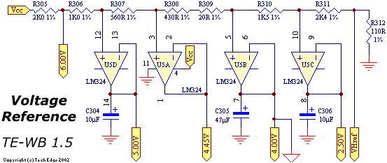
This circuit uses the 8.00 Volt Vcc signal from the previous circuit. An LM324 (U5) is set up as a buffered voltage source that is fed from a precision voltage divider comprising 1% resistors R305 through R312. This produces 4 buffered outputs of 5.0 Volts (ATtiny's Vcc), 4.45 Volts (VGnd + 450 mVolts for Vs comparison), 4.00 Volts (VGnd or Virtual Ground) and 2.50 Volts (Vstoic Reference). The voltage divider also produces unbuffered voltages of 6.0 Volts (Vs impedance check for Ip Enable) and 110 mV (VHref heater current comparison limit). C304 to C306 reduce ripple and noise on the buffered outputs. The precision resistor divider carries a current close to 1 mA when the SET 2.50 control is set correctly. |
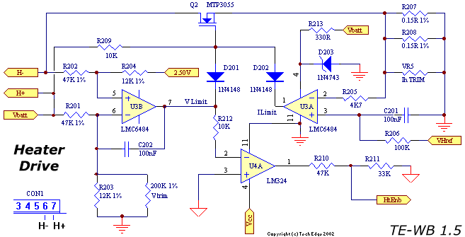
The NTK sensor's heater is driven by an ultra low dropout regulator comprising an MTP3055 (Q2) N-channel power MOSFET as the active element (minimum ON resistance of 150 millOhms) which is driven by a rail-to-rail LMC6484 quad CMOS op-amp (U3). Current (U3A) and voltage (U3B) sensing by the op-amps is combined in an OR gate pulldown mode using diodes D201 and D202.
Maximum heater current of 1.5 Amps is sensed across two 150 millOhm resistors R207 and R208 with a combined resistance of 75 milliOhms, and a voltage of 112.5 mVolts at the limit point. The actual current limit is set by the voltage across R312 (~110 milliVolts) and is just below 1.50 Amps. Some measure of heater soft start is provided by R206 (100 k) charging C201 (0.1 uF) up to the VHref value supplied by the precision voltage divider network. The Ilimit signal (pin 1 U3A) goes low any time the current limit has been reached, and acts to pull the MOSFET's gate low.
Maximum heater voltage is sensed by R201 and R202 and is set by R203 and Vtrim (200 k) to give around 10.3 Volts. The actual heater voltage is also referenced to the 2.50 Volt reference, so it is important that the SET 2.50 control is adjusted correctly. When the design heater voltage has been reached, the circuit maintains this voltage by reducing Vlimit (pin 7 U3B). This lower voltage is sensed by U4A (comparison against Vgnd of 4.0 Volts) and is used as a sign the sensor is up to temperature, and so signal HtEnb is then activated.
As the maximum working voltage of the LMC6484 is 15 Volts, D203 and R213 limit it to around 13 Volts. C202 is used for stability of the current limiter. Note that the other two sections of the LMC6484 are used in Ip Drive circuit and the WBlin linear output section. Also, although IhTRIM is not used, it is provided to enable increasing the maximum heater current IhMax.
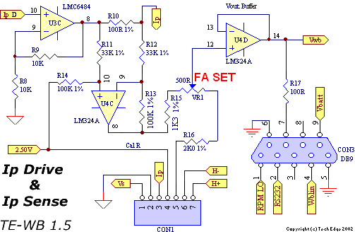
The sensor's pump cell requires a small (less than 10 mA) positive or negative current to produce its oxygen source/sink capability. The Ip drive is provided by U3C (a rail-to-rail op-amp). Ip current across the 100 Ohm R10 is sensed by difference amplifier U4C and its positive or negative output is referenced to Vstoic of 2.50 Volts set precisely by the 2.50 SET control.
The difference output voltage is buffered by U4D after a small gain adjustment set by VR1. VR1 is used to set the free-air sensor output to precisely 4.00 Volts and this accounts for small variation between sensors - even taking into account a certain amount of automatic correction made by the sensor's own calibration resistor (connected between CON1 pins 4 and 5 via the sensor cable). The 100 Ohm output resistor R17 prevents damage should the Vout signal be shorted to ground.
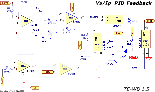
This part of the circuit, composed of a single LM324 quad op-amp U1, performs much of the sensor Vs (Voltage Sense) and Ip (Pump Current) PID (Proportional, Integral & Derivitive) feedback loop that is the essence of the sensor interface.
Buffer U1A provides a high impedance input for the narrowband Vs signal and Vs provides the error signal for the PID controller. The PID's P (proportional) term is handled by R5, the D (differential) term by C2 and R4, and the I (integral) term by C1, R3 and U1B. U1C is the P + I + D summing circuit with output IpDrive to the Ip Drive circuit describe above.
3/4 of the CD4066 quad bilateral switch U2 is used to enable/disable the IpDrive signal to the Ip drive circuit described in the previous section. Transistor Q1 is turned on, and red LED LD1 lights, when the Ip signal is anabled as described below.
When the sensor is warming up the Vs sense cell will have a high internal impedance and 100 k resistor R1 that is tied to the 6.0 Volts reference (ie. Vgnd + 2.0 Volts) will provide the drive for Vs buffer U1A. In this case U1A's output will be higher than during normal operation and even if the heater is up to operating temperature (as indicated by a low HtEnb signal), U1D's IpOff will disable the IpDrive signal from driving Ip.
When the Vs cell's internal impedance drops, it's voltage output will overcome R1's effect and U1A's output will drop from around 2 Volts to between zero and 1.0 Volts (depending on oxygen concentration). This will turn U2A ON and turn U2C and U2D OFF, and IpDrive (the PID output) will then control Ip.
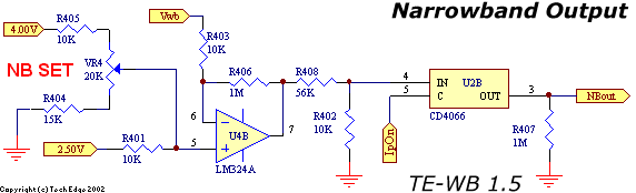
(Preliminary info) Note : either VR4 (variable NB Stoic) or R401 (fixed NB stoic) should be installed, but not both. The CD4066 simulates the high impedance of a real switching type oxygen sensor seen during warmup.
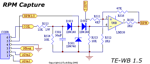
(Preliminary info) U6B is a Schmidt trigger to clean up COIL/RPM-LOW signal.
Further info ...
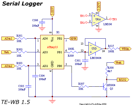
(Preliminary info) The 8 pin ATtiny15L X1 has 3 analogue input (wideband Vout, user input 1, user input 2), a digital input (RPM), and digital RS232 output, and a PWM (synthesised analogue) output. It doesn't have an external crystal and relies on an internal RC oscillator with a digital PLL. U6B is a Schmidt trigger to clean up COIL/RPM-LOW signal. U3D is a buffer for the linearized WB (0 to 5 Volt) signal. Pseudo RS232 output (0 -> 12 Volt) is from Q5. U6A is spare.
Further info ...
We appreciate your feedback on the content and any corrections necessary to this article.
Last updated 22 December 2002
Statistics by
www.digits.com
 Created 19 December 2002
| Tell me about broken links
Created 19 December 2002
| Tell me about broken links
This document is copyright © 2002, Tech Edge Pty. Ltd.
Previous |
Home |
Feedback |
Copyright