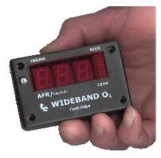
TE-5301 Wideband Display
|
This is the construction guide for the 5301 wideband fuel mixture display kit.
The 5301 is the Tech Edge version (rather than the Jaycar version) of the
modified Silicon Chip FMD design, and it features, compared to the original kit,
double sided PCBs a new front panel design,
in-built RS232 output and superbright GaAlAs 7 segment LEDs
The 5301 uses the same version 1.1 software as the 5300 and, unless noted otherwise,
is known elsewhere on this web site as the 5300 unit or the modified FMD display.
 Order a 5301 display kit from us at Tech Edge.

The rest of this article deals with constructing the unit.
Information on how to use the 5300/5301 is available here.
5301 - Construction
Note: Current 5301 kits are not shipped with the optional DB9 connector and backshell
that is required for the optional RS232 output.
|
|
Status / Errata - 19 March 2003
We are now supplying a new style socket and pin system to interconnect the top
and bottom PCBs. This makes their interconnection much more robust.
See the sections below for more information.
A small number of units have experienced problems until they have warmed.
There is a Cold fix update if this is your problem.
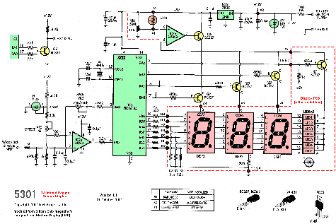
5301 Schematic
|
Click on the image of the schematic to see an enlarged version that you can save, and print.
The 5301 display is based on the Silicon Chip FMD described here.
We modified the sensor input circuitry to provide an 8 bit resolution A/D converter
between the 1.4 and 3.1 volts limits produced by the DIY-WB.
We also added the RS232 option for data logging to a Palm or PC.
|
Note that the LM336-2.5 in the 5300 has been replaced in the 5301 version with an LM431.
We also changed the 10 k resistor connected to K (cathode) of the LM336-2.5 with a 4.7 k
resistor for the LM431.
CPU (lower) Board Construction
|
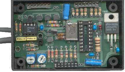
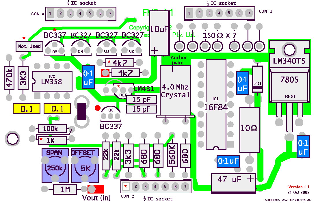
Here's an image of the lower (CPU) showing the PCB's component side.
The ribs in the case must be removed with a side cutter (and can be most easily
cleaned up with a chisel). A dremel can also be used but will take considerably
longer for the same effect.
Note carefully all the necessary changes specified in the printed guide supplied with the kit.
In particular, note the new mounting details for the LM431, the 1 k resistor,
the unused 0.1 uF capacitor, and note that the left most transistor is a BC337
(the three beside it are type BC327).
The seven 150 ohm resistors are mounted at about 60 degrees rather than vertically so they
don't foul the upper display board when everything is assembled.
|
|
|
|
Take special note of the items marked with a red asterisk.
Click on the image for an enlarged version.
We now supply a 10 and 14 pin (or some other combination to give two 7 and one 6 pin) header
sockets -- the following information (italics) is if you have an older
kit.
Note that the two 14 pin (dual wipe) IC sockets supplied in the kit must each be cut in half at both ends
and then soldered with their smooth side on the outside (the connecting part between each half
is removed as much as possible).
|
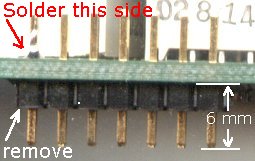
Updated header pin and socket Insertion Information
|
The image at left shows how the display PCB pins are inserted "the wrong way" for soldering.
This ensures the pin length will be about perfect at 6.0 mm (do not adjust the pins before inserting).
Take note that the black plastic is removed while the pins are still hot,
and it will simply slide off - when cold this can be quite difficult.
Note : Incorrect placement or length of the header pins can cause
lots of later problems - ensure you get this step 100% right.
To re-iterate - the pins are soldered on the COMPONENT side
(ie the "wrong side") of the PCB and the "wrong end" of the pins is soldered.
|
|
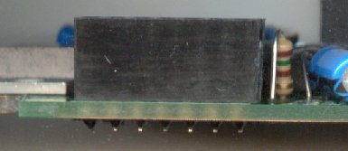
The image at right shows the corresponding header sockets on the lower PCB
(these were double wipe IC sockets on older kits).
There are no special insertion instructions except to ensure the header
is perpendicular to the PCB - check after soldering a single centre pin.
When inserted correctly, the pins and the header will mate at the perfect PCB
spacing for the two boards (~9.0 mm). See further information
below before completing this task.
|
|
|
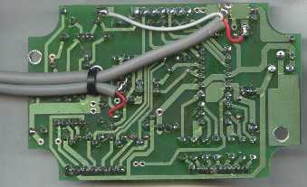
Here's the solder side of the lower (CPU) board. Note the use of the cable tie to anchor the
two cables. Top cable is power, GND and Vout (in)
Bottom cable is RS232 out and GND.
The solder mask is removed from the two cable grounding points.
Take special care not to short each cable's braid, to a PCB trace, by using
the absolute minimum of exposed braid necessary to solder to the closest ground point.
|
LED (upper) Board Construction
|
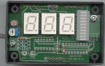
All 5301 kits are now shipped with superbright LEDs with black faces (rather
than white as shown in the image here) for higher contrast.
Here's the component side of the upper (LED) board.
Note the additional 1 k ohm resistor not found on the silk screen.
the transistor is a BC327. The resistors R1, R2 & R3 are optional 1.8 k ohm.
R2 is the calibration mode resistor.
Note the star washers under the two bolts on the component side.
The LDR (light Dependant Resistor) is rotated 90 degrees and stands off from the
PCB - it is mounted so it can be fitted through the small hole in the lid
and should then be flush with the front panel. It is better to leave it longer
and trim (or bend) the legs later.
|
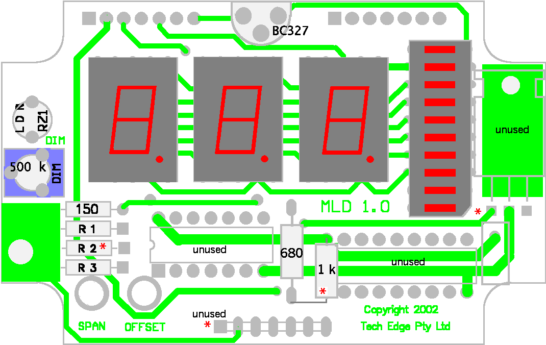
Note very carefully how the 20 pin strip is cut into two 7 and one 6 pin strips.
The 6 pin strip is used in the rightmost holes closest to the copyright notice.
The following section (in italics) has been superseded.
See the previous information if you have the header pins rather than the IC sockets.
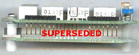
All the pins on the three strips must be pushed through as shown in the image(s) below,
this ensures the unit's two PCBs can later be successfully mated for the unit to work
and still fit into the supplied case.
|
The pins in the top board must first be pushed down so they don't protrude beyond the
black plastic retainer. The pins are then soldered from "the wrong side" or the
solder side.
The image also clearly shows the star washer and the thicker spring
washer used to correctly space the two boards. The spacer at the rear of the image
is the longer 9 mm nylon unit and doesn't use the spring washer.
|
|
|
Take special note of the items marked with a red asterisk.
Click on the image for an enlarged version.
Note that two IC sockets and a TO-220 regulator position are provided for your own
future prototype purposes - they are not used in the current design.
See the special note below regarding mounting of the LED modules to minimise
height of the PCB assembly. The trimpot and transistor should not extend past the
height of the LEDs,.
|
Special Notes
a. Minimising Total Height of LED & PCB assembly
Header Pin Mounting : The total height of the two PCBs with components must be minimised to ensure it all goes into the
case and the two boards are not stressed or bent.
The length of the pins connecting the two PCBs is minimised by pushing the pins away from
their retaining black plastic block, and soldering them so the plastic block is on the component
side of the top PCB. This technique is shown in the images above.
Bar Graph LED Module : It has stand-off legs at each corner that should be removed
with sharp side cutters before soldering.
This should now make the bar unit as high as the 3 seven segment units (no taller than 7 mm).
Extra note : The bar unit has a bevel (or chamfered) edge to indicate the pin one position. This edge can
be difficult to distinguish, but one edge will be different.

Seven Segment LED Modules :
Some models of seven segment LED modules (in particular the Agilent HDSP-5501 parts) have
stand-offs along part of their long edge. These standoffs must be removed to make them the
same height as the bar graph modules mentioned above
Extra note : The seven segment displays should be mounted
so that their decimal point is facing the center of the PCB (see above diagrams).
b. Adjustment and Calibration
The SPAN, OFFSET and DIM controls are adjusted as shown below.
Locating the controls is easy as the two PCBs have etched labels for each control.
The display PCB is wired temporarily with R2 = 1.8 k ohm (supplied in the kit),
do this simply by inserting (not soldering) the resistor no more than 1 mm
through the holes from the component side of the PCB.
After switching OFF, then back ON,
the display will now show the SENSOR INPUT voltage in volts x 10, or alternatively,
an out of range condition. You'll see either Lo, a value between
14.0 and 30.8
(representing 1.400 through 3.088 Volts), or Hi.
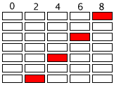
The calibration mode display actually shows 3 1/2 digits, the 1/2 digit
is the dot/bar display, and is interpreted using the image at right (note that 0 is blank).
However, as the firmware A/D converter is accurate to only 8 mVolts,
the dot/bar display will give the appearance of "jumping all over the place" as it
displays (say) 14.00 -> 14.08 -> 14.16, etc.
- the dot/bar will jump from [blank] -> 8 -> 6, etc.
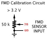 A suitable voltage source for calibration can be obtained from an external 20 or 50 k ohm potentiometer
wired across a couple of fresh 1.5 volt batteries (which should each show at least 1.55 Volts).
An accurate DVM is used to measure the voltage input to the 5301 unit
(note: leave the meter connected during calibration to
ensure the test voltage is not influenced by the meter itself).
If you have a multi turn pot, then setting the test voltage becomes easier, although this is not essential.
OFFSET Adjustment : The 5301 unit is calibrated first at a minimum input voltage of 1.400 Volts
(1400 mV) by adjusting R3, which is the 5 k ohm potentiometer (VR3 = OFFSET)
on the processor PCB (right side hole). The display should read 14.0 and the dot/bar should be blank.
Ideally, the OFFSET pot should be set to almost display Lo as this will be closest to 1400 mV.
SPAN Adjustment : For the other end of the range, it is calibrated at a maximum input voltage of 3.000 Volts
by adjusting the 200 k (or 250 k) ohm potentiometer (VR2 = SPAN) on the processor PCB (left side hole).
The display should read 30.0 and the dot/bar should be blank.
Ideally, the SPAN pot should be set to almost display 29.9 as this will be closest to 3000 mV.
This procedure should be repeated as each adjustment may slightly affect the other.
A quick check at other points in the displayed range of 1.40 to 3.08 can be made, but remember
the DVM you use may have some linearity errors as well as the FMD circuit. The two
displayed voltages should track such that the rightmost FMD digit is never off by more than one
from the DVM's corresponding displayed value.
DIM Adjustment :
This is difficult to do other than at night and in the vehicle itself. An approximation
can be made by slipping a black pen cover over the LDR (out of the case) and adjusting the
DIM control to just blank the display, and then turning the control a fraction to just turn it
back on.
c.5301 Display Interpretation

|
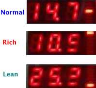
The display's three basic regions of operation are shown at left.
- A normal operating value (of 14.7 in this case)
is shown as three digits. The display's normal range covers
from a rich of 10.0 through to stoic of 14.7 and to a lean of 24.9.
- An over rich condition is shown as 10. followed by an
equals or less than symbol (=<). Note that an AFR of lower than 10 can occurr momentarily
when the accelerator is backed off rapidly and the injectors have built up a
reserve of fuel (this is often followed by a very lean DFCO condition)
- An excessivly lean condition is shown as 25.
followed by a greater than or equals symbol (>=).
This condition can occur normally on EFI vehicles when the ECM turns off the
injectors to save fuel during deceleration (known as DFCO, or deceleration fuel cut-off)
|
5301 Parts List
ABS black plastic case (see note 0)
FMD 1.1 (16F84 processor, lower) PCB
MLD 1.0 (LED display, upper) PCB
16F84A-4/P (pre-programmed, -20/P may be supplied)
LM358
LM431 (see note 1)
7805 (or LM340T5)
1N4746A
BC327 x 4
BC337 x 2
HDSP-5501 x 3 seven segment LED (see note 2)
HDSP-4820 10 LED array (see note 2)
4 Mhz Xtal (a mini version may be supplied)
LDR
10R 1W 5% (note: R = ohms, W = Watts, k = 103)
150R x 8 (all 250 mW 5%, note : 4k7 = 4.7 k))
680R x 4
1k0 x 2 (see note 3)
1k8 x 2 (see note 5)
3k3 x 2
4k7 x 2 (see note 1)
22k x 2
100k
470k
560k
1M
5k trimpot (5 mm) note : marking = 502
200k or 250k trimpot (5 mm) note : marking = 204 or 254
500k trimpot (5 mm) note : marking = 504
15 pF x 2 NPO ceramic
0.1 x 4 block mono (deep blue colour)
0.1 x 2 polyester (yellow colour)
10 uF electro
47 uF electro
Header strip x 20 pin male (see note 4)
8 pin DIP socket (dual wipe)
6 + 7 + 7 header pins, (see note 6)
18 pin DIP socket (dual wipe)
Cable tie x 2
DB9S female DB9
DB9 shell and mounting parts
2 m two core shielded wire
M3 15 mm x 2 phillips head bolts
6.3 mm x 3 threaded nylon bush
9 mm threaded nylon bush
M3 star x 2 washers
M3 spring washer
M3 6 mm x 2 countersunk bolts
- note 0 : The case is a standard ABS plastic case that is
specially processed with a laser cut printed lid
and red acrylic laser cut insert.
- note 1 : LM431 replaces LM336-2.5 but requires special
insertion as the pin-outs are different. Additionally, the 10 k resistor
we originally specified for connection to the LM336's cathode is
changed to 4.7 k when the LM431 is used.
- note 2 : Alternative super-bright LEDs may be supplied.
Also, see the construction guide regarding trimming the LED's mounting stand-offs.
- note 3 : one of the 1 k resistors is used on the top
(display PCB) and is not on the silk screen layout
- note 4 : the header strip is cut into 2 x 7 and
one 6 pin strip.
- note 5 : the 2 x 1.8 k resistors are for calibration and
optional modes (discussed in the text). Don't solder in R2.
- note 6 : The two 14 pin DIP socket (dual wipe) have been superseded by
header sockets that may be supplied in a combination that will give at least a six (6)
and two seven (7) pin headers.
Last updated 19 March 2003 (header pins)
Previous |
Oz DIY-WB Home |
Order Oz DIY-WB parts/units |
Copyright

 Statistics by
 www.digits.com
Shows approximate unique hits since 17 July 2002.
This document is © Copyright Peter Gargano 2002
Previous |
Home |
Feedback |
Copyright
![]() Order a 5301 display kit from us at Tech Edge.
Order a 5301 display kit from us at Tech Edge.
![]()


 A suitable voltage source for calibration can be obtained from an external 20 or 50 k ohm potentiometer
wired across a couple of fresh 1.5 volt batteries (which should each show at least 1.55 Volts).
An accurate DVM is used to measure the voltage input to the 5301 unit
(note: leave the meter connected during calibration to
ensure the test voltage is not influenced by the meter itself).
If you have a multi turn pot, then setting the test voltage becomes easier, although this is not essential.
