These notes should help you construct your own TE-WB version 1.5 (and 1.1)
NTK (UEGO) oxygen sensor interface unit. Please read all text before you start
as there are many procedures you should perform in sequence.
Modifications Required to the PCB
Firstly inspect your PCB for any shorts between adjacent tracks.
Although we have very few problems of this nature, they are always
best to find before you've built the unit, and as we use sockets,
it's sometimes difficult to find shorts afterwards.
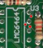
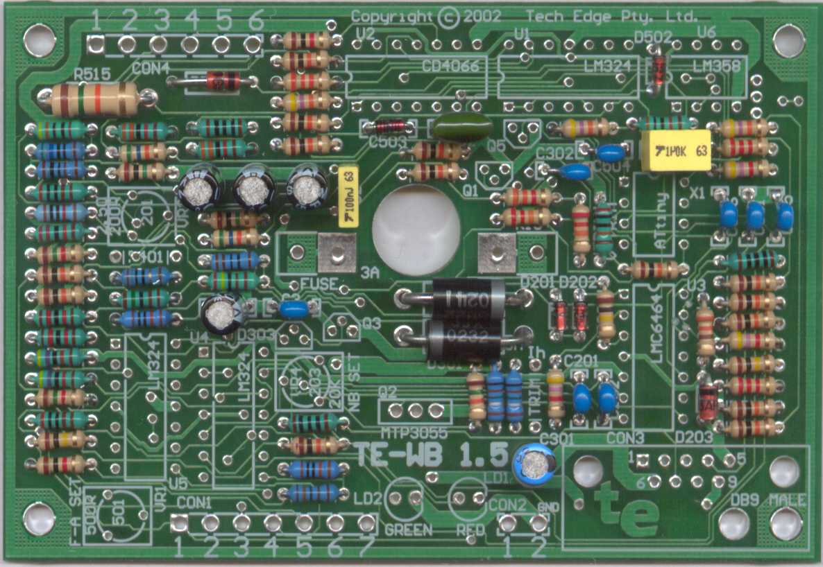
You should find three tracks have been "drilled out", these are shown in
the image at left as RED dots.
Note also that the marking on the PCB is
incorrect as you will have been supplied with an LMC6484 rather than 6464.
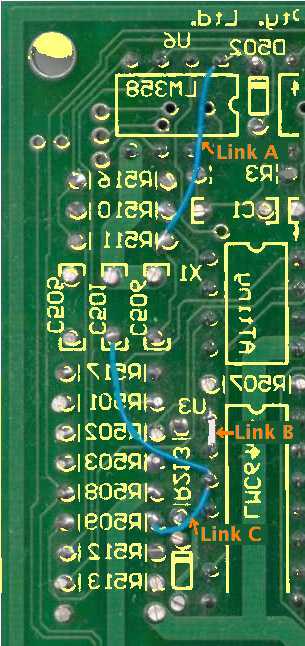
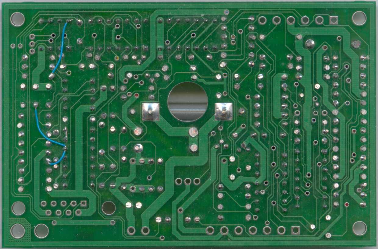
This composite image shows the solder side of the PCB with the silkscreen
from the other side superimposed on it (that's also why it's reversed!).
You'll need to use the supplied wire (thin PVC or Teflon coated wire wrap wire)
to connect 7 points on the PCB. Use two pieces of the wire and strip and cut it as
you solder link A to two points and link C to three points.
link B doesn't need any insulation as it's between two adjacent pin (13 and 14 of U3).
Click on the image for an enlargement.
Note that this operation should be performed after all other components have been soldered.
We mention it here as this operation reconnects the cut links (above) to their correct points.
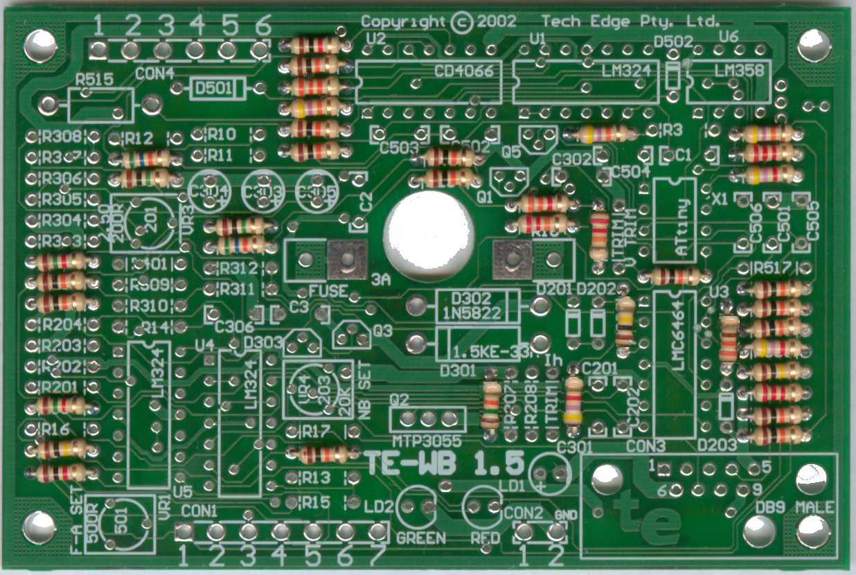
If you haven't already done so, you should go here and
print off a colour copy of the component location(s).
Note the silkscreen has visual cues for using 1% or 5% resistors with the 1%
resistors having a dotted line as shown in the blowup at right.
It is important that 5% resistors are not used where a 1% resistors is called for.
But it's okay to use a 1% in place of a 5%.
We may actually substitute a 5% with 1% in the parts kit from time to time,
but we will never substitute a 1% for a 5%.
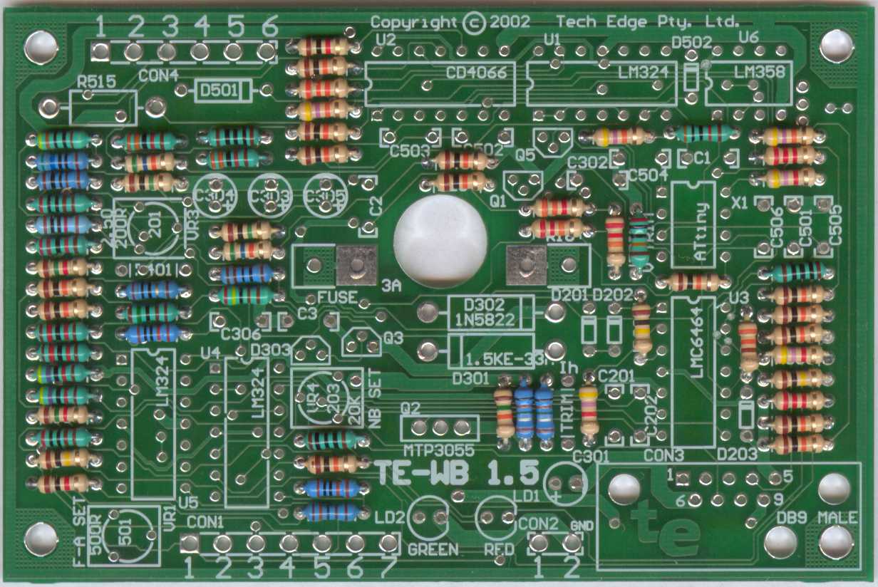
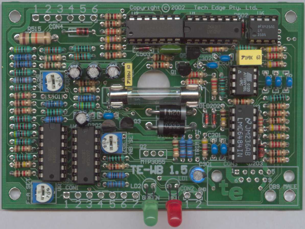
First we insert the physically lowest components - these are the resistors, and
we have inserted just the 5% resistors first as these are more numerous.
The 5% resistors will all have just 4 coloured bands with an extra gold band indicating
the 5% tolerance.
5% resistors typically have a beige or light brown background.
It's best to orient them with the gold band to the right and to the top so
the values can be most easily read from left to right and bottom to top as
the silkscreen is printed.
Note two 5% resistors should be left out.
These are R401 (narrowband fixed stoic option)
and TRIM Ih (default IhMax is very close to 1.5A).
Next the 1% resistors go in.
Note that VTrim (just to the left of the 8 pin ATtiny socket) is
shown as using a 5% resistor, but we have used a 200 k value that is only
available in a 1% version.
At this stage we have all the 1% and 5% 1/4 watt resistors in place.
We can now put in the capacitor, both electrolytic, polyester,
and block monolithic, as well as the diodes and the remaining 5% 1 Watt
resistor (R515 = 15k).
Make sure you get the orientation of the diodes and electrolytic capacitors correct,
and make sure you don't mix up the 1 Watt zener diodes D203 and D501.
Lastly - put in the IC sockets noting that their pin 1 indent is correct (to the left or top).
Put in the LEDs making sure the base of the LED is close to 9 mm from the PCB (tip
of LED is then about 19 mm from the PCB.
Then any remaining components like the fuse holder tabs and the potentiometer.
Take special note to make sure the pots are NOT pressed "too far"
into their holes as their leads' sharp "stops" can short out onto the PCB traces beside.
Push in and then pull the pots back out 1 mm before soldering them.
If you didn't read down to here before you started (as we suggested),
you probably had trouble putting in C1 (large yellow 1.0 uF capacitor)
along with R3 and the ATtiny 8 pin socket, so we suggest you do those three
parts all at the same time (so leave R3 and C1 until you do the sockets
near the end).
Don't forget you have to put in the three jumpers as described at the start.
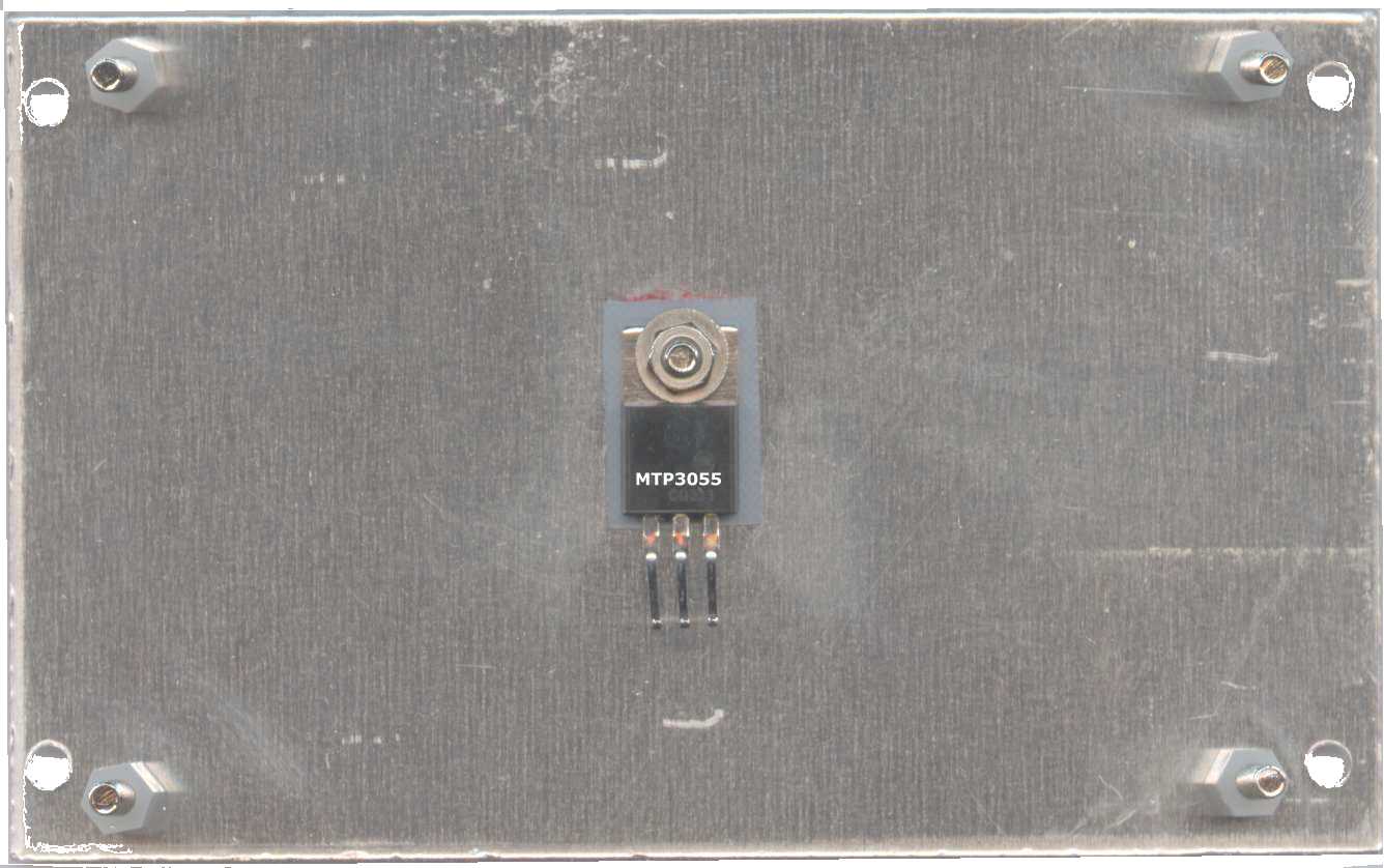
The heatsink must be prepared for the PCB by first attaching the four 6 mm
nylon standoffs using four 15 mm M3 bolts. The PCB should now be a snug fit
into these 4 bolts - but don't attach the nuts (with star washers yet) as
we have to attach the MTP3055 MOSFET (which is static sensitive, so you
should observe static sensitive procedures).
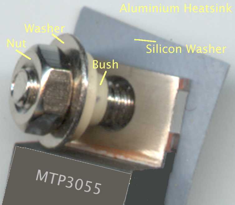
The TO220 heatsink insulation components are mounted in the following order :
10 mm M3 bolt thru' the heatsink, grey silicon washer, MTP3055, beige washer,
flat steel washer, M3 Nut.
Make sure the MTP3055's legs are bent at 90 degrees to fit into the
three holes designated "MTP3055" on the PCB.
The next few paragraphs details how the wire leads are attached to the PCB and to the plugs/connectors.
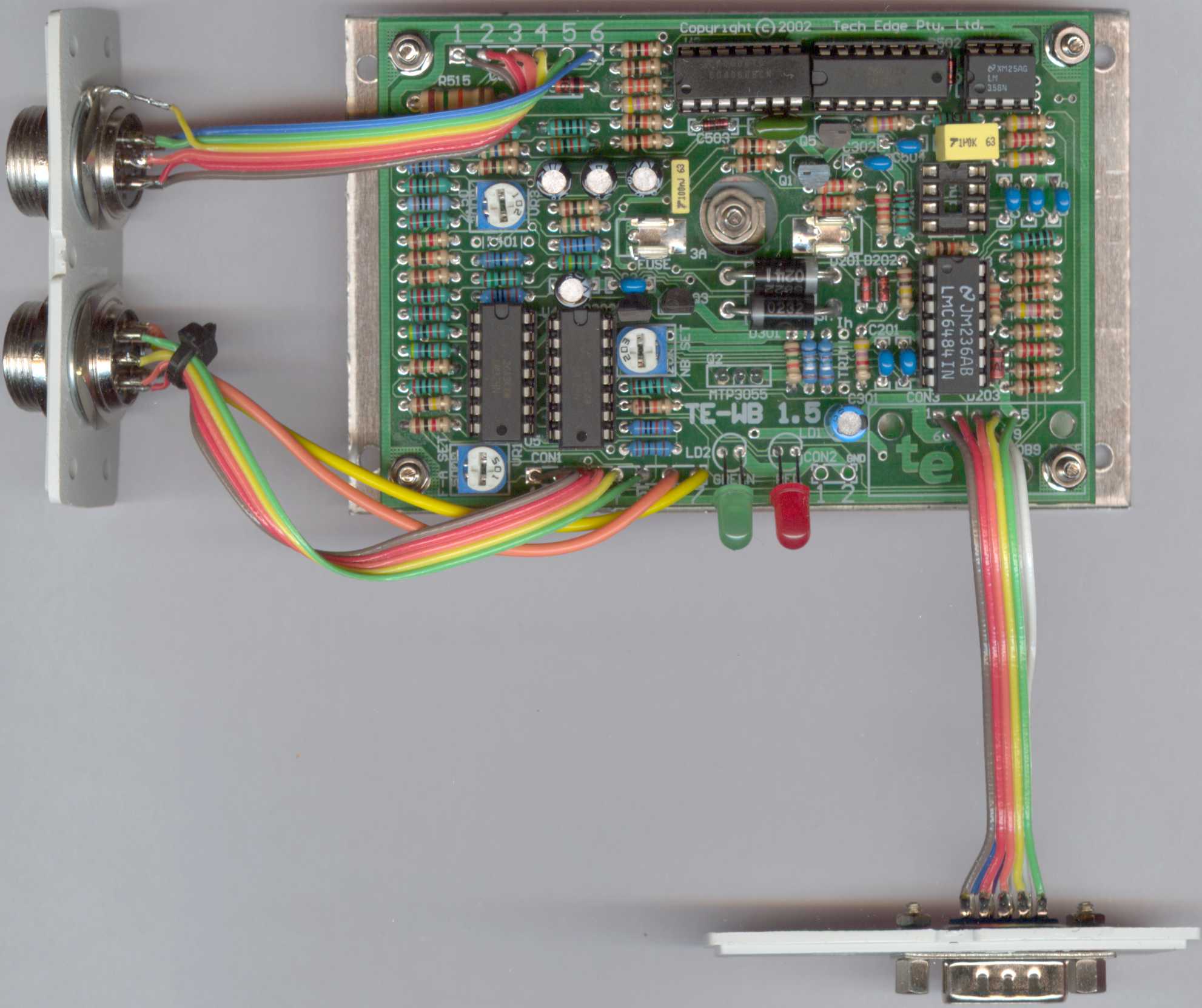
Here's an image of the unit with leads attached to the PCB. Note that the
two thicker wires go to CON1 pins 6 & 7.
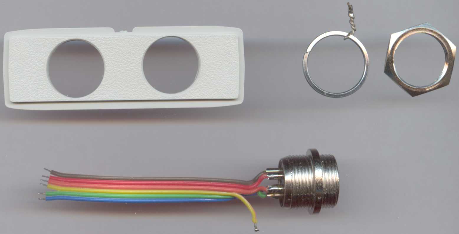
The parts shown here make up the end of the wideband case that holds the two
connectors - one for the NTK sensor cable,
and the other for the data acquisition cable.
These connectcors are described below.
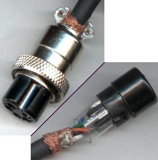
Note that the 5 pin socket uses the socket's body as an earth pin to make it a 6 way connector.
The length of tinned copper wire must be soldered to the washer to create a "tab".
The washer is used under the nut holding the 5 way circular connector to the end plate.
The "tab" is also shown side on in the enlarged image of all the unit's leads above.
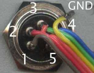
This is how the circular 5 pin connector is wired.
Note that the yellow conductor is wired to the "tab" described above.
The ribbon cable colours match the right side composite image below showing CON4 on the PCB.
Note that the circular connectors have small numbers beside each pin for positive identification.
CON4 Pin
Ribbon Wire Colour
5 pin Circular connector
Usage
Name
1
Brown
1
user ADC input #1
ADin1
2
Red
2
user ADC input #2
ADin2
3
Orange
3
Narrowband 0-1v output
NBout
4
Yellow
"tab"
Signal Ground (Shield)
Gnd
5
Green
4
RPM Pulse input (5v)
RPM LO
6
Blue
5
RPM Coil input (12v)
COIL
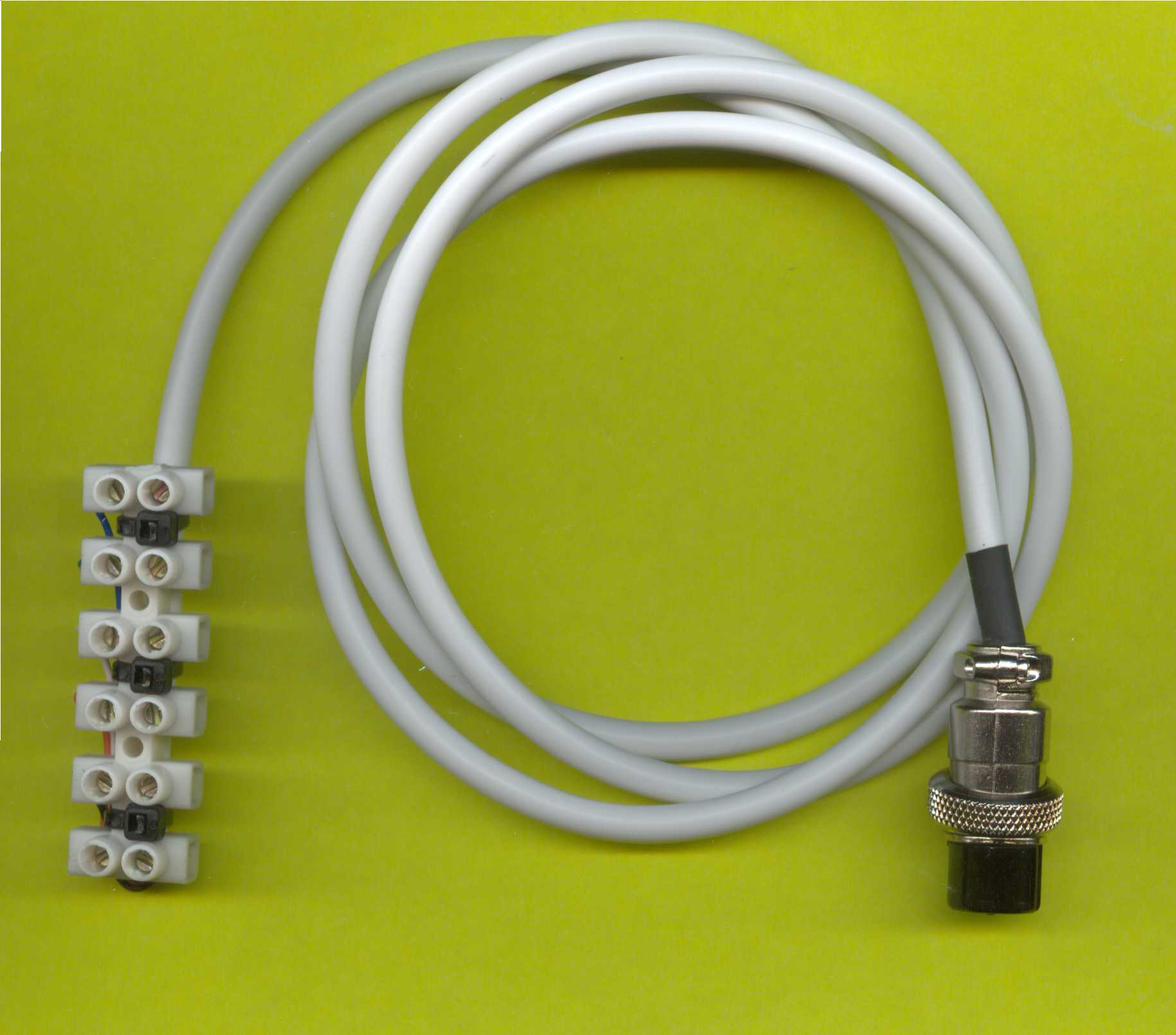
The data acquisition cable (or D/A cable) mates with the 5 pin circular
connector and has a 6 pin terminal block at its other end.
Click on the image for an enlargement.
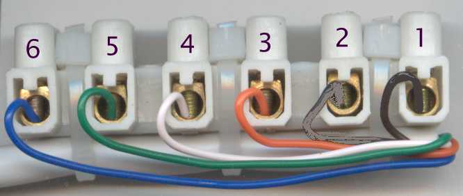
The following table shows how to wire each end of the D/A cable.
Note that the white coloured lead is connected to the shell of the plug
but as the shell doesn't have a specific "lug" to solder to, we
used some solder wick wrapped around the cable, and soldered the white
wire to it. This can be seen here.
5 pin Plug
Wire Colour
Terminal Block Pin
Usage
Name
1
Black
1
user ADC input #1
ADin1
2
Brown
2
user ADC input #2
ADin2
3
Orange
3
Narrowband 0-1v output
NBout
Shell
White
4
Ground
Gnd
4
Green
5
RPM Pulse input (5v)
RPM LO
5
Blue
6
RPM Coil input (12v)
COIL
The composite image shows how CON4 on the PCB matches the 6 pin terminal block when everything has been wired correctly.
This is how to wire CON1 to the circular 8 pin connector.
Note that wires to pins 6 and 7 are heavier duty, the othre 5 wires a light ribbon cable.
CON1 Pinout
Wire Colour
8 pin Circular connector
Name
Usage
1
Brown
1
Vs
Sense Voltage
2
Red
2
Vs/Ip Common
Virtual GND
3
Orange
3
Ip
Pump Current
4
Yellow
4
RCal ref
RCal Ref (2.5 Volts)
5
Green
5
RCal
Calib. Resistor
6
Orange
6
H-
Heater -
7
Yellow
7
H+
Heater +
Further information
Please refer to the Debugging Section for construction common problems.
Note: More information (but for the version 1.0 WB unit)
can be found here. We're still
migrating some of that information to this guide ....
We appreciate your feedback on the content and any corrections necessary to this article.


 Created 22 December 2002
|
Created 22 December 2002
| 